
Tungsten probes are commonly used for wafer testing due to several advantageous properties that make them suitable for this application:
Hardness: Tungsten is one of the hardest materials available, and this hardness helps in maintaining the sharpness of the probe tips. This is crucial for making precise and accurate contact with small features on semiconductor wafers.
High Melting Point: Tungsten has a very high melting point, making it resistant to melting or deforming at the high temperatures often encountered during wafer testing processes.
Electrical Conductivity: Tungsten is an excellent conductor of electricity. This property is vital for ensuring good electrical contact with the semiconductor devices on the wafer.
Chemical Inertness: Tungsten is chemically inert, meaning it does not easily react with other chemicals or materials. This is beneficial in environments where the probes may come into contact with various substances during testing.
Wear Resistance: Tungsten is known for its wear resistance, which is important for maintaining the longevity and performance of the probes over time, especially when making repeated contact with semiconductor wafers.
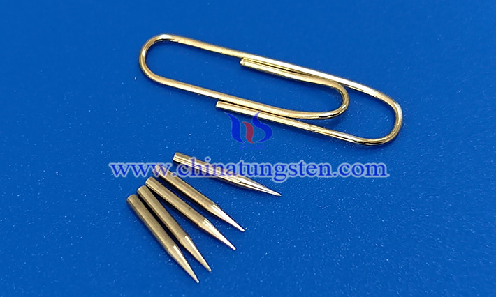
Thin Diameter: The tungsten-made probes can be manufactured with very thin diameters, allowing for precise and non-destructive testing of small features on semiconductor wafers without causing damage.
Stiffness: Tungsten-made probes can be designed to have the right balance of stiffness, allowing them to penetrate surface layers and make reliable electrical contact without being too rigid or too flexible.
These properties collectively make tungsten probes well-suited for the delicate and demanding task of wafer testing in the semiconductor industry. The ability to provide accurate electrical measurements without damaging the wafers is crucial for quality control and performance assessment during semiconductor manufacturing.
Chinatungsten Online is a professional manufacturer of tungsten and molybdenum for nearly thirty years. We can supply various kinds of tungsten needles as per the drawings. Please free feel to contact us when you got the purchasing plans.


